Chipus launches a battery charger IP in a 0.18 µm BCD process
BCD (BIPOLAR-CMOS-DMOS) is a key technology for power ICs. This combination of technologies brings many advantages: Improved reliability, reduced electromagnetic interference and smaller chip area.
The power management section of ICs for portable applications often requires low power consumption together with high voltage operation capability, which leads to big challenges for IC design with respect to power consumption and chip power dissipation.
As this requirement has become crucial in today’s market demands, Chipus has updated its portfolio with a battery charger IP (CM1712ff) using a BCD technology that assures the coexistence of high-density logic and high voltage devices, giving origin to a new set of features with configurable specifications.
The silicon proven IP (CM1712ff), features:
- Configurable 100mA to 1.1 A fast charge current
- 100mA/500mA USB modes
- 30V tolerant input
- Integrated power FET and sensing
- Integrated regulator for external loads
- Internal OTP memory for factory and user configuration

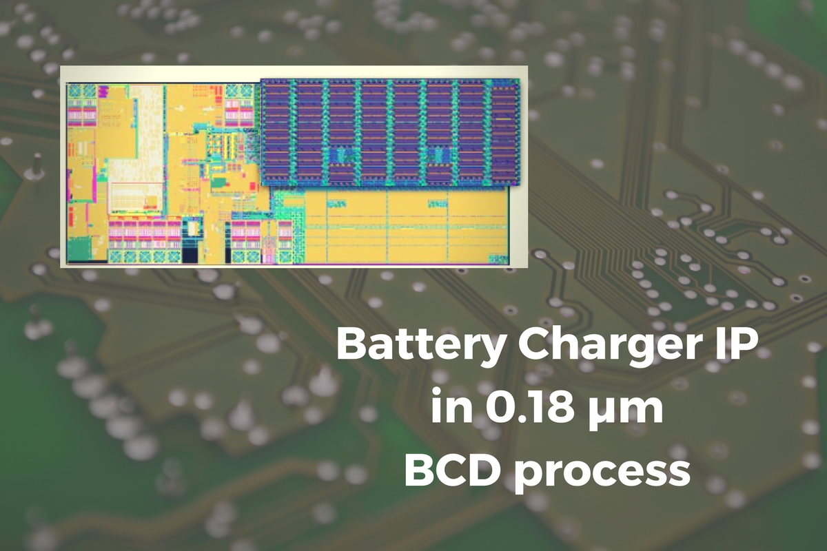
Layout of Chipus Battery Charger highlighting the power DMOS device
“We launched our first battery charger IP in Silterra C18GH5, which is a 5V technology. Now, we are launching an improved version using a BCD process, making it possible to make the circuit tolerant to input voltages as high as 30V”, says Daniel P. Mioni, IC Design Leader at Chipus. “This is an important increment to our IP and IC design services offering in Power Management, mainly due to the high demand for high-voltage tolerant applications enabled by BCD processes”, says Murilo Pessatti, Chipus’ CEO.
With the use of the BCD technology in the battery charger IP, Chipus seeks to guarantee high quality and reliability in all types of application environments. The reliable coexistence on the same chip of low-voltage control circuits and high-voltage DMOS stages with typical voltage capability, opens the door for uncountable applications. With this achievement, Chipus looks to continue capitalizing their innovative products, develop more tailor-made solutions to their customers, allowing them to match their specifications in a shorter design cycle.
About Chipus
Chipus Microelectronics is a semiconductor company specialized in the development of low-power, low-voltage, analog and mixed-signal intellectual property (IP) blocks for integrated circuits (ICs) and systems on chip (SoCs). It develops configurable IP core architectures that allow a good level of customization together with high IP portability, providing unique level of freedom on customer design requirements. Chipus is headquartered in Florianopolis – Brazil, with a Sales office in Santa Clara – California and a Sales Representative in Europe.


