Ultra Low Power Oscillator Design Considerations (<70nW)
Florianópolis, Brazil — June 30th, 2021
When designing circuits and systems for battery powered devices it is imperative to consider the power consumption as a key design parameter to be minimized. There are actions to be taken on System, Circuit and Device level to minimize the consumption of the chip.
Before going into the specific characteristics of the oscillator…
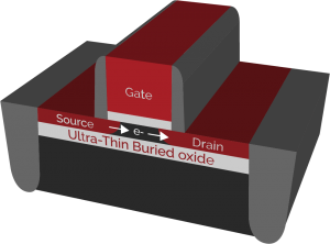
It is important to discuss the process that was used to design it: the FD-SOI process. This acronym stands for Fully Depleted Silicon On Insulator and it finds use in applications that require high digital performance along with low power analog circuits. In this process, there is a buried layer of oxide that insulates the transistor from the substrate, reducing leakage and parasitic capacitances. The thickness of the transistor channel above the oxide layer is small enough so that the channel does not require doping, thus is fully depleted. This technology has some exploitable advantages, such as low current leakages and the flexibility of controlling the device threshold by changing the voltage at the substrate, without the issue of any diode entering in conduction. A simplified cross-section of a transistor is shown in Figure 1.
Figure 1 : simplified cross-section of transistor in FD-SOI process
In the context of a Power Management ASIC in which the customer has particularly strict consumption requirements, the oscillator designed to perform the clock management has to be equally economic as this block is kept running for most of the time. This project required an Ultra Low Power Oscillator that delivers a 1MHz (± 10%), 0.8V using only 50nA in 22nm FD-SOI process, in typical conditions. It is biased by a 5nA current sink and features a 4 bit digital bus to perform calibration and an enable digital input to shut down the entire block.
In order to achieve this consumption level
It is necessary to bias the circuit with the least possible current, since it goes through a current mirror, where the calibration happens. This mirror has a selectable ratio to compensate for process variations on the output frequency.
Most of the variability on this circuit comes from considerations on the bias current variability, in particular with respect to temperature. As a System design choice to reduce consumption, the current reference was not compensated with respect to temperature, rendering a process variation in the bias current of ± 7% and a temperature variation of ± 25%. However, the precision specs of the block are still met with this bias that is proportional to temperature.

Figure 2: Simplified schematic of the Ultra Low Power Oscillator.
The last but not least, the Level Shifter
Since the current through the core is minimized, consequently, so it is its voltage output swing. This imposes on the NMOS part of the Level Shifter the need for a tiny threshold voltage, to respond to the core output. This is performed by a careful selection of the device used and usage of adequate body biasing techniques. Having the transistor channel isolated from substrate allows to use the bulk connection as a back-gate, effectively changing the threshold voltage as shown in the schematic of Figure 2.


